Field Programmable Gate Arrays, or FPGAs, are electronic devices that allow designers to program digital circuits. They have become a popular solution for complex applications, especially in industries such as telecommunications, aerospace, and defense. This article will provide an in-depth understanding of FPGA technology, its architecture, and its applications.
What is an FPGA?
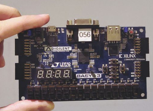
An FPGA is a semiconductor device that allows users to program digital logic circuits. FPGA Chip Unlike Application-Specific Integrated Circuits (ASICs), FPGAs do not have a fixed circuitry that is pre-designed and manufactured. Instead, they have programmable logic blocks, configurable interconnects, and programmable I/O blocks. With these programmable elements, users can design custom circuits and implement them on the FPGA.
FPGAs have several advantages over traditional ASICs. One significant advantage is that FPGAs are reprogrammable, which means they can be programmed multiple times. This flexibility allows designers to modify their designs quickly, which is essential in applications where time-to-market is critical.
Another advantage of FPGAs is that they are highly customizable.
Designers can choose the logic blocks, interconnects, and I/O blocks to suit their specific requirements. This customization results in a highly optimized design that can be tailored to meet the exact needs of the application.
FPGA Architecture
FPGAs consist of three main components: programmable logic blocks, configurable interconnects, and programmable I/O blocks. The logic blocks and interconnects are the primary elements that allow users to design custom circuits.
Logic Blocks
The logic blocks are the building blocks of the FPGA. They contain configurable lookup tables (LUTs) and flip-flops. LUTs are used to implement Boolean functions, and flip-flops are used to store and synchronize data. The LUTs and flip-flops are interconnected to create combinational and sequential circuits.
The LUTs in a logic block are typically 4-input or 6-input, which means they can implement any Boolean function with up to four or six variables, respectively. The output of the LUT can be fed to a flip-flop, which can be used to store the output or synchronize it with other circuits.
Interconnects
The interconnects are the wires that connect the logic blocks. They are configurable and can be used to create any routing path between the logic blocks. The interconnects can also be used to create buses, which are groups of wires that carry data between circuits.
The interconnects in an FPGA are usually segmented into multiple levels.
The first level connects the input and output pins to the logic blocks, while the higher levels provide connections between the logic blocks. The segments are programmable, which means they can be configured to create any routing path between the logic blocks.
I/O Blocks
The I/O blocks are used to interface the FPGA with external devices. They contain configurable input and output buffers, which can be used to interface with various types of devices. The I/O blocks can also contain configurable termination resistors, which can be used to match the impedance of the external devices.
FPGA Design Flow
The design flow for an FPGA involves several steps, including design entry, synthesis, placement, routing, and bitstream generation.
Design Entry
The design entry involves creating a high-level description of the digital circuit using a Hardware Description Language (HDL) such as VHDL or Verilog. The HDL code is used to describe the functionality of the circuit, including the inputs, outputs, and internal signals.
Synthesis
The synthesis step involves translating the HDL code into a gate-level netlist. The netlist is a list of logic gates and their interconnections that implement the functionality described in the HDL code.