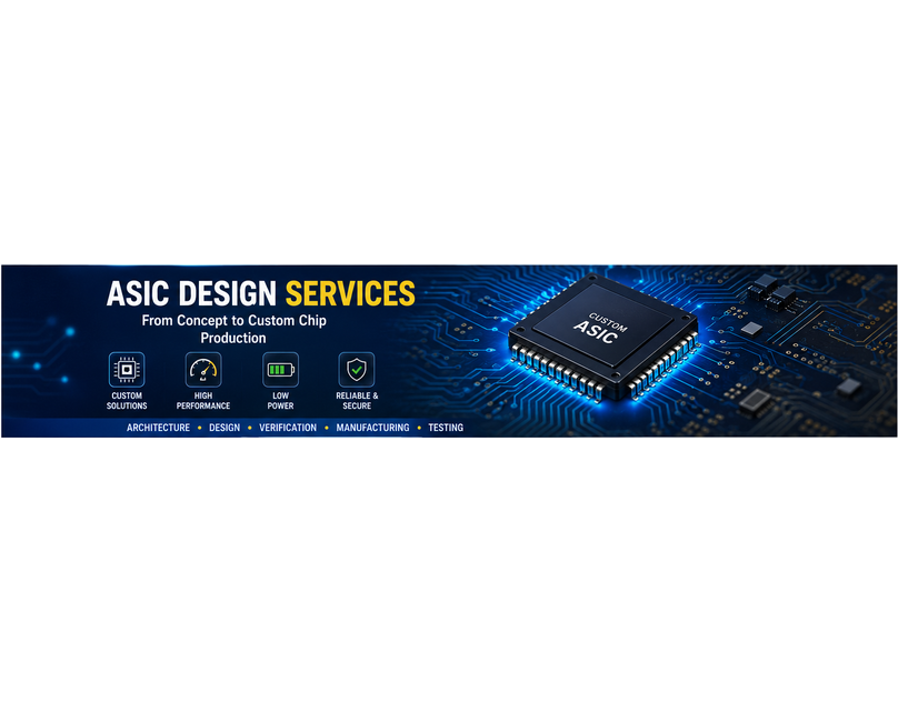
ASIC design services help companies create custom chips for specific product requirements. ASIC stands for Application-Specific Integrated Circuit, which means the chip is designed for a dedicated function rather than general-purpose use.
Many businesses choose custom ASIC design when standard off-the-shelf components cannot meet their needs for performance, power, size, cost, reliability, or long-term product availability. From medical devices and industrial sensors to communication systems, automotive electronics, and signal processing products, ASICs can help improve product performance and reduce system complexity.
However, ASIC development is a detailed process. It requires experience in architecture, analog design, digital design, layout, verification, manufacturing, packaging, and testing. That is why working with a trusted IC design company or professional ASIC design house can make the project more efficient and reduce technical risk.
What Are ASIC Design Services?
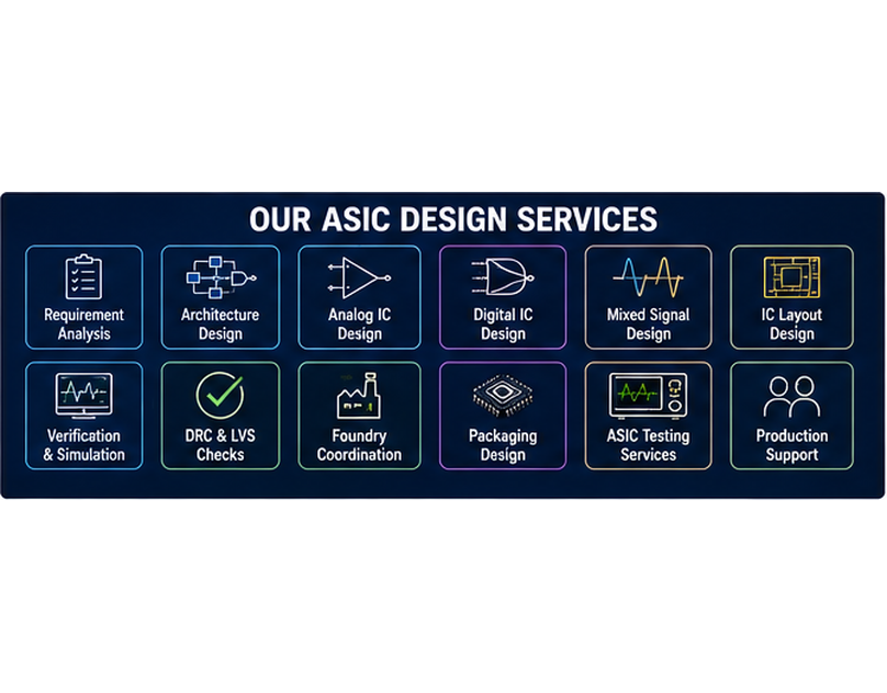
ASIC design services include the complete technical support required to design and prepare a custom chip for manufacturing. These services may cover the full development flow or only specific stages, depending on the project.
A complete ASIC design service may include:
- Requirement analysis
- Feasibility study
- System architecture
- Analog circuit design
- Digital IC design
- Mixed signal ASIC design
- IC layout design
- Design verification
- ASIC simulation
- DRC and LVS checks
- Foundry coordination
- ASIC packaging
- ASIC testing services
- Production support
A company may need a full turnkey ASIC design solution or support for only one part of the process, such as layout, verification, or testing.
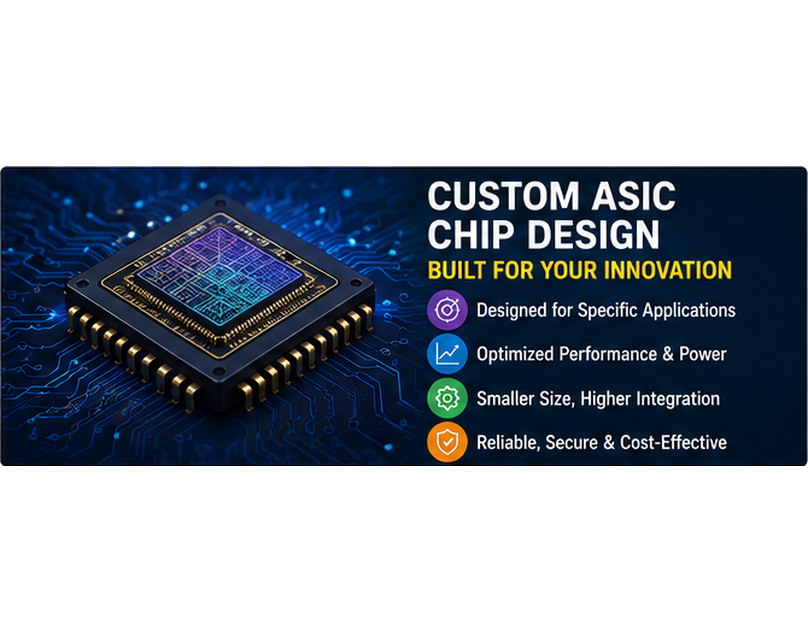
Why Companies Choose Custom ASIC Design
Custom ASIC design is useful when a product needs a chip that is optimized for a specific application. Standard components may work for early prototypes, but they may not be ideal for long-term production or high-performance systems.
Companies often choose ASIC design services to achieve:
- Lower power consumption
- Smaller product size
- Better signal performance
- Higher reliability
- Reduced board complexity
- Improved manufacturing consistency
- Lower unit cost at high volume
- Better intellectual property control
- Long-term component availability
For example, a sensor product may need a custom analog front end, ADC, and digital control logic inside one chip. A medical device may need low-noise signal capture with strict reliability. A communication product may need high-speed signal processing and low-power operation.
In these cases, professional ASIC chip design can provide a more suitable solution than using multiple standard chips.
Step 1: Requirement Analysis and Feasibility
The ASIC design process begins with understanding the product goals. Engineers review the application, signal requirements, performance targets, power limits, package size, cost goals, and production volume.
This stage helps answer important questions:
- What function should the chip perform?
- Does the design need analog, digital, or mixed signal blocks?
- What are the power and performance targets?
- What process technology is suitable?
- What package type may be required?
- What testing approach will be needed?
- Is a full custom ASIC justified?
A strong feasibility study helps avoid costly mistakes later. It also helps decide whether the project needs fabless ASIC design, a full turnkey chip design services approach, or only selected design support.
Step 2: Architecture and Design Planning
After requirements are clear, the next step is architecture planning. This stage defines the main blocks of the chip and how they will work together.
The architecture may include:
- Analog front-end circuits
- Digital logic blocks
- ADC or DAC blocks
- Memory blocks
- Power management circuits
- Clocking circuits
- Communication interfaces
- Built-in test circuits
Good architecture is important because it impacts chip area, power, speed, cost, manufacturability, and reliability. A skilled ASIC design house will plan the design in a way that supports both performance and production requirements.
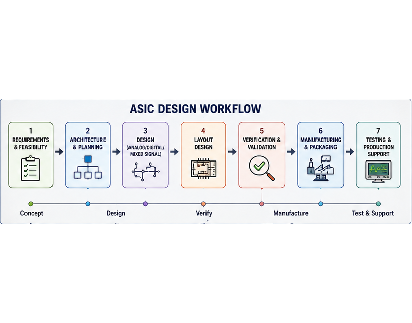
Step 3: Analog, Digital, or Mixed Signal Design
Once the architecture is approved, engineers begin detailed circuit design. Depending on the application, the chip may require analog IC design, digital IC design, mixed signal ASIC design, or a combination of all three.
Analog design may include amplifiers, filters, voltage references, current mirrors, ADC input stages, and sensor interfaces. Digital design may include logic, control blocks, registers, memory interfaces, or signal processing circuits.
Mixed signal design combines analog and digital sections on one chip. This is common in sensor ASICs, medical device ASICs, industrial control systems, and signal processing ASICs.
At this stage, simulation is used to check whether the circuit performs correctly before moving into layout.
Step 4: IC Layout Design and Physical Verification
IC layout design is the physical implementation of the chip. It defines how transistors, wires, blocks, and connections are placed on silicon.
Layout is especially important because physical placement can affect noise, signal integrity, power consumption, timing, and reliability. In analog and mixed signal ASICs, poor layout can create mismatch, interference, and unstable performance.
Physical verification includes checks such as:
- DRC, or Design Rule Checking
- LVS, or Layout Versus Schematic
- Parasitic extraction
- Timing verification
- Power integrity checks
- Signal integrity checks
These checks confirm that the design is manufacturable and matches the original circuit intent.
Step 5: ASIC Verification and Simulation
Before tapeout, the design must be carefully verified. ASIC verification confirms that the chip will perform correctly across different operating conditions.
Verification may include:
- Functional simulation
- Analog simulation
- Mixed signal simulation
- Timing analysis
- Corner analysis
- Monte Carlo simulation
- Power analysis
- Post-layout simulation
This step helps reduce the risk of fabrication failure or costly redesign. Strong verification is one of the most important parts of professional ASIC design services.
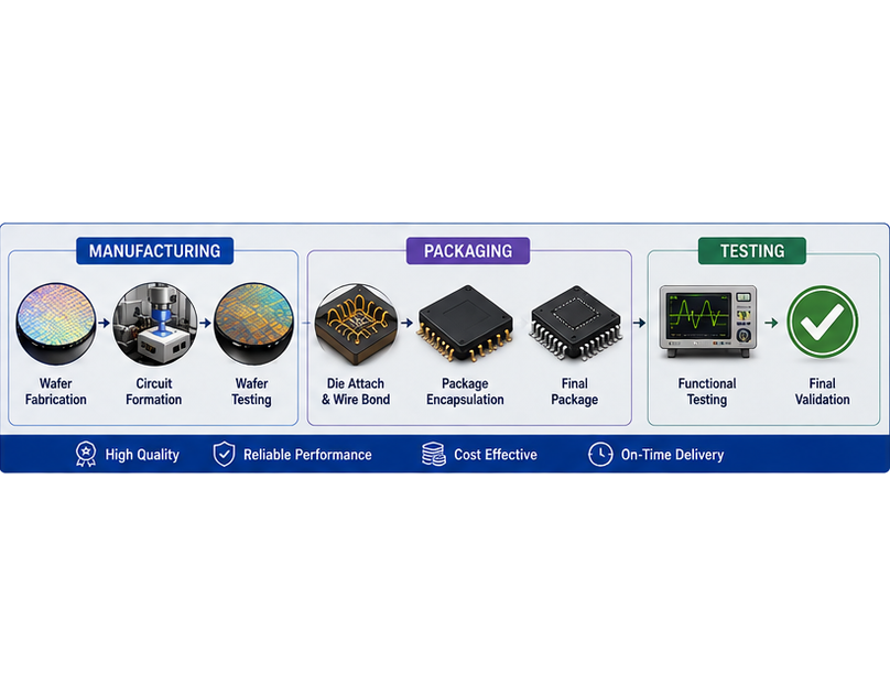
Step 6: Manufacturing, Packaging, and Testing
After the chip design is verified, it moves to tapeout and manufacturing. During ASIC manufacturing, the chip is fabricated on a silicon wafer by a semiconductor foundry.
After fabrication, the chip is packaged. ASIC packaging protects the silicon die and provides electrical connections for integration into the final product.
The final stage is ASIC testing services. Testing confirms whether the manufactured chips meet performance, reliability, and production requirements.
ASIC testing may include:
- Wafer-level testing
- Functional testing
- Electrical testing
- Temperature testing
- Reliability testing
- Production test development
Testing is essential because it helps detect defects and confirms that the chip performs correctly in real-world conditions.
What Is Turnkey ASIC Design?
Turnkey ASIC design means the full chip development process is managed from concept to production. This may include architecture, design, layout, verification, foundry coordination, packaging, and testing.
A turnkey ASIC design solution is useful for companies that want one experienced technical partner to manage the complete chip development flow. This can simplify communication, reduce project delays, and improve accountability.
Businesses that do not have an internal semiconductor design team often choose turnkey chip design services for full project support.
How to Choose the Right ASIC Design Company
When choosing an ASIC design company, look for experience in your application area and technical requirements.
Important factors include:
- Experience with analog, digital, and mixed signal ASICs
- Strong simulation and verification process
- IC layout design expertise
- Foundry and packaging knowledge
- ASIC testing support
- Clear development workflow
- Ability to support production scaling
- Experience with similar industries
The right IC design company should not only design the chip but also help reduce risk throughout the complete development cycle.
Conclusion
ASIC design services help companies develop custom chips that match their exact product requirements. From early feasibility and architecture to circuit design, layout, verification, manufacturing, packaging, and testing, each stage plays an important role in chip success.
For businesses building advanced electronics, working with an experienced ASIC design house, IC design company, or turnkey ASIC design partner can help improve performance, reduce system complexity, and bring reliable custom silicon to production.